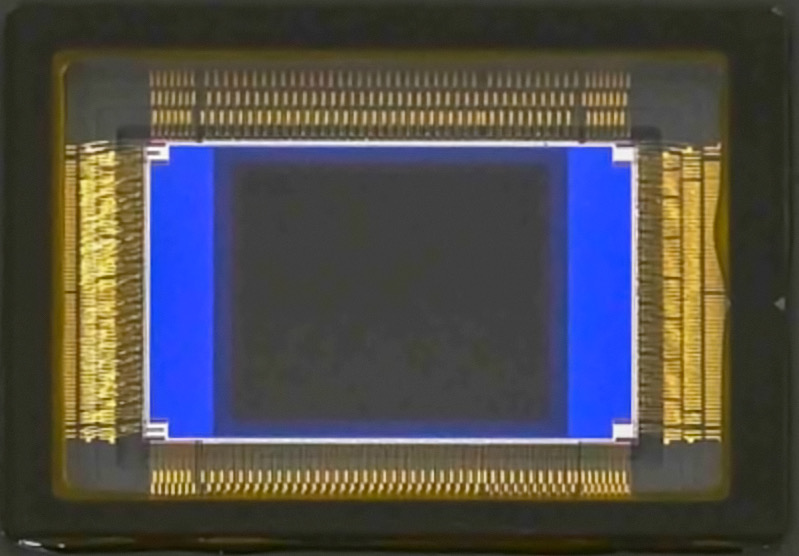
Curiously, after being mostly quiet on the scholarly conference circuit, Nikon has returned this week with a presentation at the International Conference on Solid State Circuits (ISSCC). Even more curious is the sensor Nikon describes.

Would you believe an 18mp, 1", BSI-stacked CMOS sensor capable of 1000 frames a second, HDR-type dynamic range extension (to 134dB, or 22+ stops engineering DR), and a pixel size of 2.7 square microns? The experimental chip described was apparently fabbed on a 65nm stepper, which is generally smaller than being used for large sensors at the moment.
Why 1"? Probably for economical reasons. You don't want to start sophisticated sensor development with full frame because to do that requires multiple stitching passes on the stepper, and we have two different layers (image portion, and stacked portion) already being dealt with. In other words, solve one problem at a time. But more importantly, it appears that Nikon might actually have created this sensor specifically for industrial use, which would be a new market for them (they currently don't supply such sensors that I know of).
The presentation describes new technology that appears to be derived from one of the four Nikon sensor patents I've been following.
Hopefully this will bring to rest the notion that Nikon doesn't have a sensor design group. They do. It's active, and has been active since 1988.
What any of this means for dedicated cameras is unclear. However, the fact that Nikon is dabbling in multiple advanced sensor technologies isn't a fluke. They've been doing that for as long as I can remember, they just tend to do it quietly ever since the D2h "fiasco."